At Microbritt, we specialise in the development and manufacturing of materials used in the semiconductor industry and quantum technology. Our underlying patented technology relies on the processing of materials routinely used in the semiconductors industry. This enables us to create custom architectures that are otherwise impossible to achieve.
We work with a range of sizes, from small die to 12-inch wafers. Our technology also allows the post-processing of materials fabricated by other means to give enhanced capability.
A gear to prove our capabilities! Use Microbritt to fabricate your complex design, easily.
Advanced Through Silicon Holes / Vias
Shallow, to deep high-aspect ration holes / vias in Silicon
High-precision hole drilling up to a thickness of 10 mm for specialist applications. Minimum hole radius – 25 microns. Capability offered in a range of materials.
Glass Silicon Complex Structures
Glass / Silicon Through-Hole Vias
Microbritt Customer-defined Products
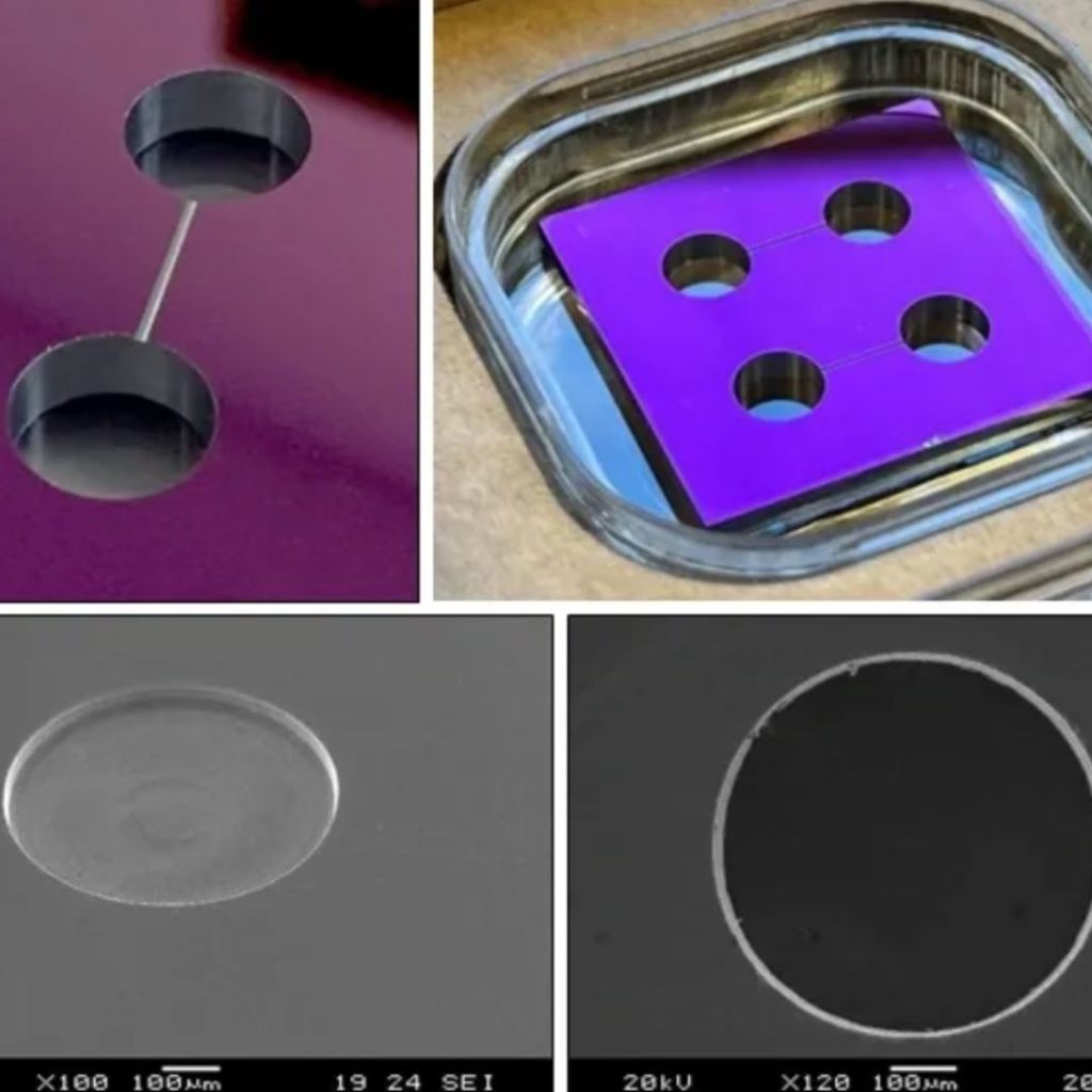
Suspended Microstructures
Suspended Silicon Bridges
Bridge dimensions: 200 micron wide, 200 micron deep. (Note: not the limit of our capability)
Speak to our expert team
Have any questions about our services? Drop us a line.
Our Service
Ready to send your designs? Visit our fabrication portal…
SEND US YOUR DESIGN
Receive a quote & delivery date. This includes prototypes and low value, high value items.
RAPID MANUFACTURE
The product will be manufactured with our patented process.
RAPID DELIVERY
Your product will be rapidly delivered to anywhere in the world